Generally speaking, when motherboards die they die for a good reason. Once you get to the point where you’ve checked every RAM slot, reset the BIOS, removed all peripherals fans and accessories, swapped CPUs and it STILL doesn’t come to life then chances are you’re in trouble.
I took this on as an exercise as up to this point I had never actually sat down and tried to bring a motherboard back from the dead. On that note, I’ve never had a modern (post 2005) motherboard completely fail to show signs of life.
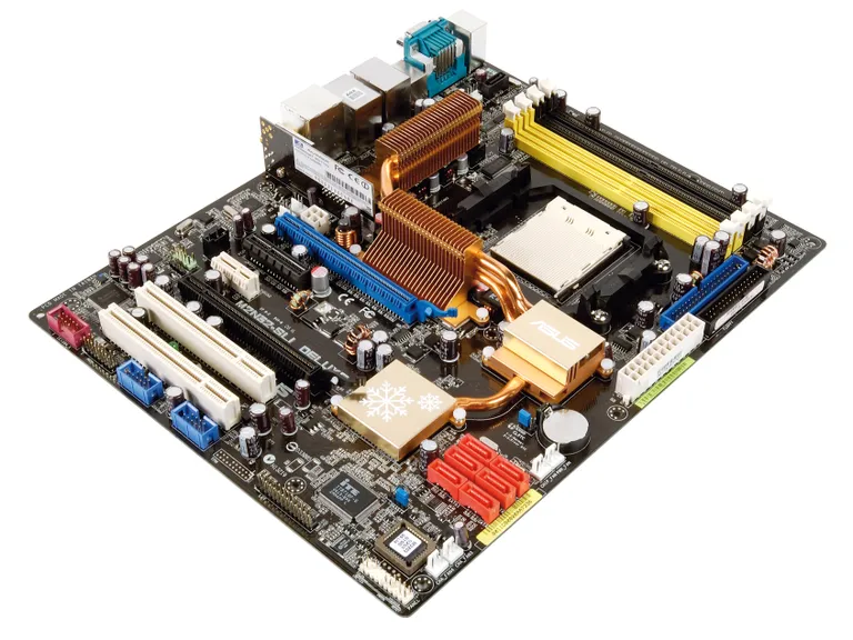
The motherboard in question is based on nVidia’s nForce 500 chipset, specifically the nForce 590 which boasts features such as full 16+16 lane SLI, 6x SATA 3Gbps ports, 10x USB 2.0 ports and support for dual RAID 5 configurations. This board has most of those features, and even includes some extras like dual gigabit ethernet, built in 802.11b/g Wi-Fi, and a whole host of legacy and modern I/O ports.
Now, as far as I know, a static discharge to one of the front USB ports seems to have been the most likely culprit in taking out this board. The details are foggy, but that is what I’m going off of.
Doing a power test of the board results in the CPU fan spinning up and the standby LED remaining illuminated. The CPU itself remains cool to the touch, as do the CPU voltage regulator FETS. The northbridge and southbridge chip on the other hand do seem to be alive and get quite warm, prompting me to put a heatsink on the southbridge.
I did the basic troubleshooting steps just for the sake of sanity. I swapped the CPU out, tried a couple different sticks of RAM and RAM slots, swapped multiple GPUs into both PCI express slots, reset the BIOS, but it was clear it was more than just a basic hardware issue.
I took a photo of the board from above and used Paint.NET to label all the obvious power devices such as voltage regulators and MOSFETS, as well as their pinouts.
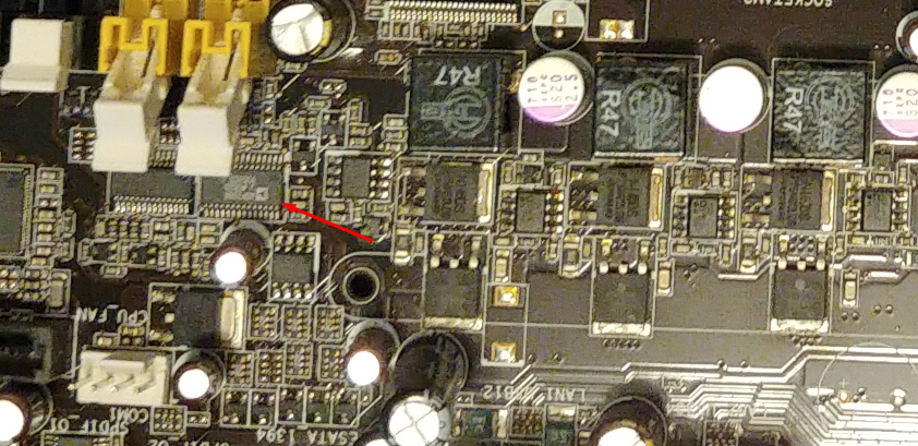
Nothing seemed particularly unusual as first. Regulators were regulating, power rails seemed within reason, but that CPU was still cold which made me focus on the MOSFETs responsible for providing it with the precisely regulated core voltage. I checked a few ICs and came across this fella tucked away near two of the memory slots. As can clearly be seen it reads ADP3186, which is, and I quote:
“a highly efficient multiphase synchronous buck switching regulator controller optimized for converting a 12 V main supply into the core supply voltage required by high performance AMD processors.”
That seems important!
Thanks to the wild web a datasheet is readily available, and below is a pinout of this particular IC:
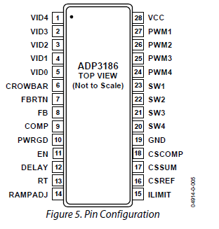
The datasheet also explains the startup sequence and what conditions may cause it to cease operation. The most basic requirement for this IC to even think of doing anything is that the EN pin has to be pulled high, which never happens. I suspect the EN pin is driven by the north or southbridge, but being as they’re BGAs, trying to trace that back wouldn’t be easy, or even possible, so I took a look at another IC first.
The other IC in question is the IT8712F Super I/O chip which handles several legacy devices like floppy drives, parallel and serial ports, and hardware monitoring such as temperature and voltage monitoring, as well as fan control. It’s also responsible for triggering the PSU to turn on and off when the power button is pressed (and held), which is working.
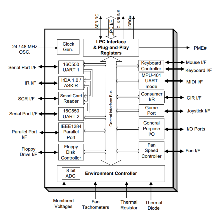
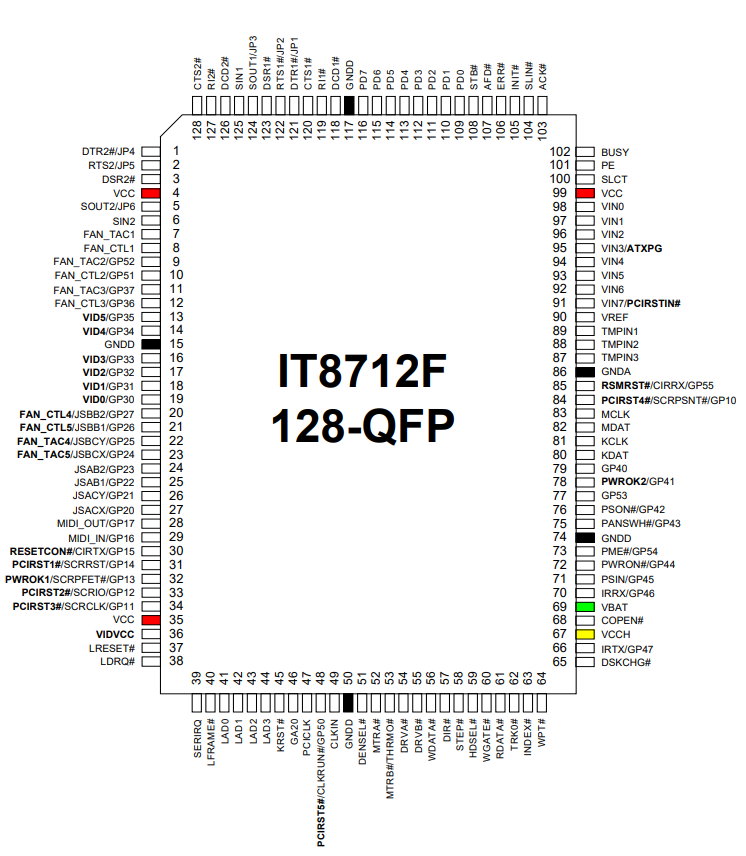
I thought perhaps this chip was also responsible for triggering the EN signal of the CPU buck controller but it doesn’t seem to be that simple. I probed around and took a look at some signals, only to find it’s not getting a required clock signal on pin 49, nor is it getting a PCI clock on pin 47, and the !RESET is being pulled low.
Judging by the board layout the clock signal should be coming from the southbridge, as there are no nearby crystals or oscillators. And without a clock this chip isn’t doing much of anything, except for triggering the PSU to turn on and off, which must be it’s own dedicated circuit.
My best guess at this point is the southbridge took a hit since the front USB 2.0 ports are routed straight to into it. There are dedicated transient voltage suppressors connected to each +/- USB data pin which test fine when forward biased using a diode test. The unfortunate thing about ESD events is the damage tends to be invisible. An IC stops working suddenly and there’s no obvious explanation. This seems to be the case here but I could be wrong and am always welcome to comments on the subject.