For the longest time I never had a proper variable bench power supply. One reason being they seemed very expensive for what they do, or at least for what I needed. There are the questionable Chinese ones in the $100 range which have adequate specs if you’re willing to take the risk, or you can spend considerable amounts of money on something from a reputable manufacturer. Most the time I never desperately needed one, and in a pinch a standard ATX PSU with 12/5/3.3/-12V rails worked well enough. Those few cases where I did need an adjustable voltage left me longing for a proper bench supply, and would usually lead me cobbling together something crudely on a breadboard for temporary use. I decided it was simple enough a project to do myself, and so I began searching for the parts I needed to make it happen.
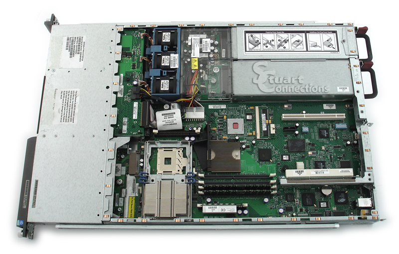
Being into electronics and PC repair means I have a lot of junk perfectly good albeit obsolete hardware laying around. One of these is an old HP ProLiant DL360 G3 1U server which itself is powered with a pair of redundant 460W power supplies. Given that this thing mostly just turns electricity into noise these days, I didn’t feel bad scavenging the PSUs. The supplies themselves are made by Delta Electronics, which is a very reputable power supply manufacturer. Specs are shown below:
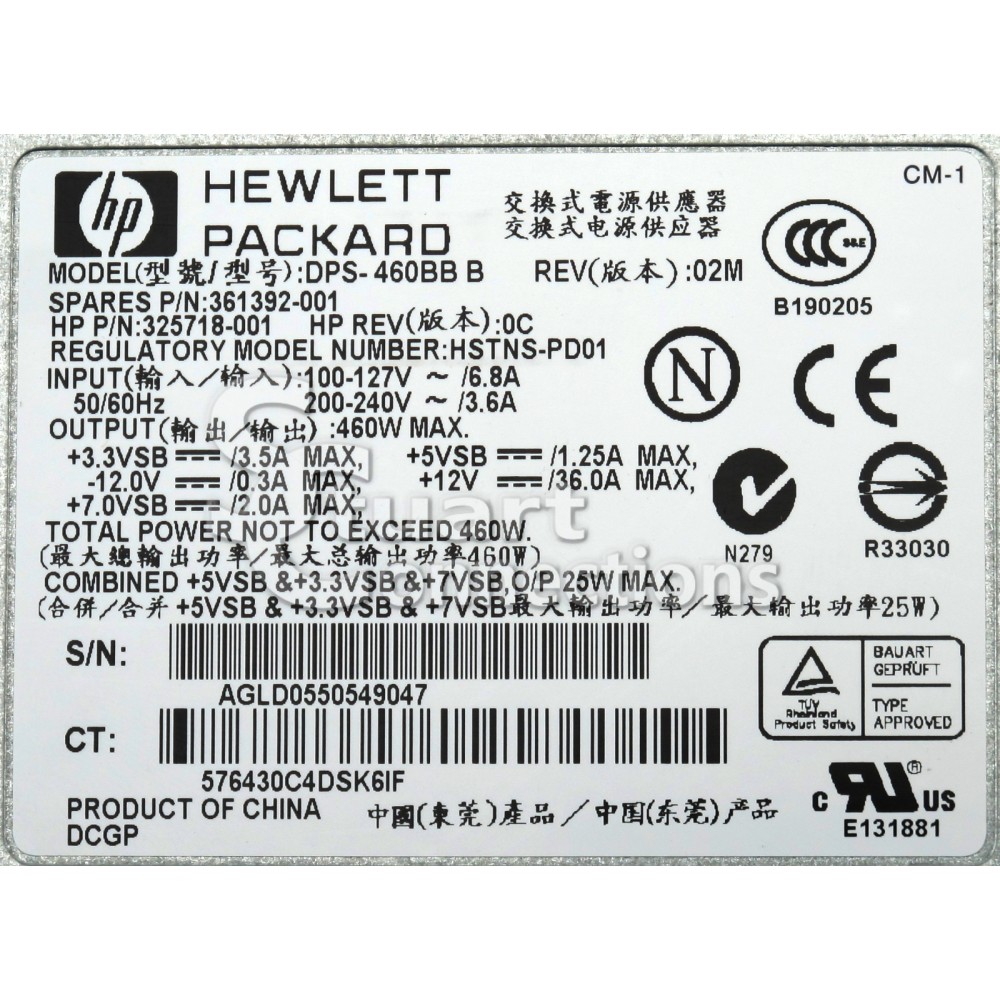
The PSU’s themselves have several rails, including -12V, 3.3V, 5V standby, 7V, and big meaty +12V rail capable of 36A, giving 420W on that rail alone. 12V is a somewhat low upper limit for bench work, but the high current capabilities were appealing.
Requirements:
The requirements for the design are fairly simple:
- Current and voltage control
- Constant voltage and constant current mode
- Output on/off switch
- Output isolated from chassis earth
- Relatively accurate current and voltage readout
- Ability to output more than 12V (Say 15 to 20?)
Determining Pinout
So where does one start with a project like this? There’s certainly no schematic available for these, making the level of difficulty fairly high right off the start. This also means there’s no obvious way of powering them up. The PSU’s have a card edge connector on the ends, which allows them to slot in and out of the server while running for minimal down time.
Without even powering them up, we can start to determine what the purpose of several of the connectors are by using a multimeter and some logic.
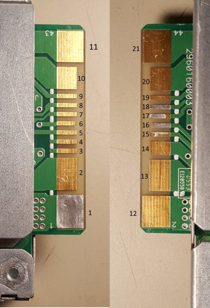
In this case and most cases, it helps to figure out which pins connect to ground. The chassis of these PSU’s are tied to the output ground, and with a quick check we find that pins 1, 11, 12, 21 and 6 are grounded.
Next, we can find which contacts are connected to one another by checking for continuity from one pin to each remaining pin. Doing this, we end up finding several shorted pins: 2, 10, 13 and 20. Seeing as the 12V rail is designed to 36A, and these 4 contacts are very large, it would be safe to assume this is our 12V rail.
Lastly we can look for pins which are visibly not connected to anything, and here that would be pins 3 and 4.
Since I have the server these PSU’s mate with, I’ll be plugging them in and reading the pin voltages both when the server is powered off and on. This will show all the differences between each pin and should allow one to determine which pin or pins are responsible for actually powering it on.
The connectors that the PSU’s slot into contain 2 rows of 28 pins, entering the mainboard at a right angle. Only the middle 22 of the 28 pins are utilized. Using a spreadsheet to record the values, I simply probed each pin on each row and entered the voltages with the server off (but in standby) and powered on.
Most pins showed their expected values, but pins 16 and 18 dropped from 5V to 0V during power up. I pulled the PSU back out and tried grounding pin 16 and 18 individually and found that it wouldn’t power up properly unless they were both pulled low. So with that figured out, the following chart shows the known pin out of the PSU:
| Pin | Function | Pin | Function |
|---|---|---|---|
| 1 | GND | 12 | GND |
| 2 | +12V | 13 | +12V |
| 3 | NC | 14 | +3.3V |
| 4 | NC | 15 | +5V |
| 5 | LED_ON | 16 | PSU_ON (Active Low) |
| 6 | GND | 17 | -12V |
| 7 | (Voltage Control?) | 18 | PSU_ON (Active_Low) |
| 8 | (Protection trigger?) | 19 | +7V |
| 9 | (Current monitor?) | 20 | +12V |
| 10 | +12V | 21 | GND |
| 11 | GND |
The functions of pins 7, 8 and 9 are uncertain and derived from the schematic which will be shown later in this post.
What Now?
At the moment we know how to turn it on, and we could stop there if that’s all was required. There are many applications where a high current fixed +12V PSU are useful. One such use would be to pair this with a DPS30xx or 50xx step-down power supply module:
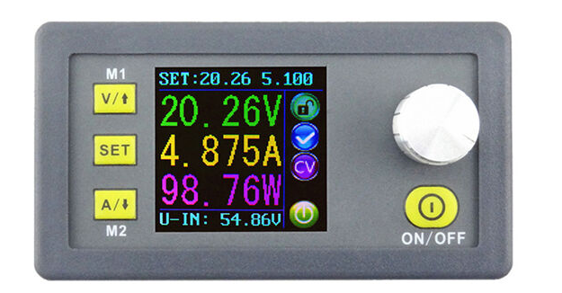
In fact I would recommend anyone attempting something like this to stop here unless you have a lot of time and patience. The above module can be found in several variations for around $15 to $50USD depending on the current/voltage handling capabilities. They offer voltage and current control in a neat and tidy package and all they require is a power supply that can supply about 10% over the maximum voltage you require.
Voltage and Current Control
Being a regulated power supply, the internal circuitry is continuously monitoring the output voltage to ensure it stays at a fixed value. If a load on the output causes the output voltage to drop, the voltage generating circuits will react and compensate by increasing the output voltage until the original value is obtained. This is known as negative feedback.
A power supply of this nature will also be monitoring the output current to ensure it stays below an upper limit. Beyond that limit, some kind of protection will kick in to prevent damage to the load, itself or both. Ideally, for the sake of this project, the protection will be in the form of the output voltage dropping until a steady current is achieved.
In both cases, the fixed value that the output voltage and current are being compared to are some kind of precision voltage references. The reason for using a precision reference is that they are stable over a wide range of temperature and input voltages, meaning the reference and therefore our output does not drift with changes in temperature or fluctuations in say the AC line voltage.
But in our case we actually want the reference to change, or rather, we want to be able to change it ourselves. If we can find the references and make them adjustable with a simple potentiometer, our power supply’s output will follow the changing reference thereby making it adjustable, which is one of our major requirements.
Taking a look inside
As there is no schematic to speak of, and we require one to be able to modify the existing circuitry, we must make one ourselves. The first step is opening it up and seeing what we have to work with.

This is a very tightly packed design. Power comes in on the left and the regulated output exits on the right. The large pink rectangle is a silicone thermal transfer pad for utilizing the case as an additional heatsink. The white part is some kind of insulating sheet which wraps around the entire underside of the PCB which is designed to insulate the high voltage circuitry from the chassis.
The copper plate is additional heatsinking for the output devices and also makes contact with the chassis. This important as it will later need to be isolated from the chassis if we want the entire supply to be an isolated design.

Looking at it from the end, it’s clear how densely packed it is as is the nature of the 1U height restriction. To say it requires forced airflow is an understatement; You would need to pound the air with a hammer to force it through this thing. But to anyone who’s ever heard the shrill of a 1U server power cycling would have no doubt those tiny 40mm fans are fully capable of doing such a job.
Further removing the insulating sheet and copper heatsink, we are greeted with…more heatsinks. And some liberal amounts of thermal compound.

I’ve jumped the gun slightly before this photo was taken and desoldered the long riser PCB which spanned the high voltage side. More to come on that later. But for now, let’s see what we can figure out just by looking at this.
Basic Switchmode Topology
If we want to be able to find our reference and tap into it, we need a basic understanding of what’s happening on the circuit level. All well designed and safe switchmode power supplies have a very similar topology to the diagram below:
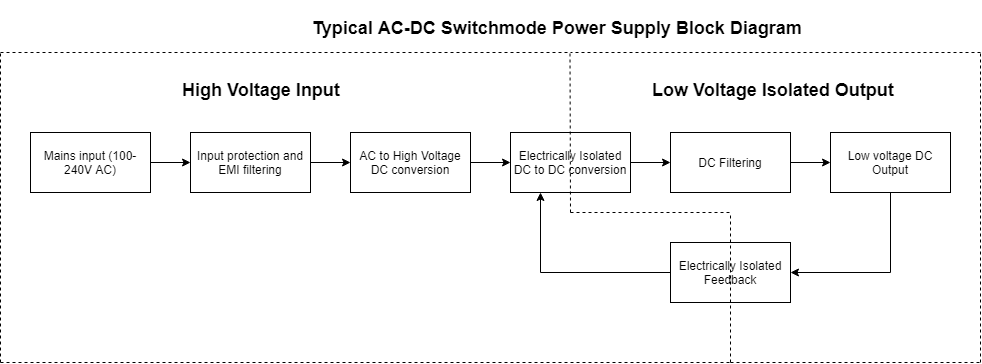
Electrically isolated, or often referred to as galvanic isolation, means there are no conductors or semiconductors connecting the output to the input side. There may be transformers, capacitors, or opto-isolators, but nothing through which current can flow directly. The reason for this is safety. If some catastrophic event occurs on the input side, for example a lightning strike, the supply is designed so that the lethal arc never makes its way to the human using the device.
If we take a close look at the underside of this PSU, there is a clear physical separation running the width of the board where no trace passes. Above this layer sit two large transformers which being magnetically coupled devices also have physical separation of the conductors.

But somewhere, the output voltage and current and possibly other signals must cross this barrier so the control circuitry knows whats happening on the output side.
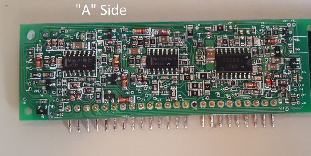
There is one auxiliary PCB which bridges the gap from the high voltage to the low voltage side, and I have already desoldered it as mentioned previously:

There is a lot going on here, but there is also clear separation from the left and right side with the exception of 4 identical devices stacked in a column, near the middle-left of the PCB. These 4 legged devices are called opto-isolators. They are analog devices which utilize photons emitted from an internal LED to control a phototransistor on the other side. This allows information to be sent from one side of the package to the other without making electrical contact and therefore maintaining electrical isolation.
Knowing about how switchmode power supplies work, it’s safe to assume these are responsible for feeding the voltage and current and other information back to the control circuits and this would be the best place to start making a schematic.
The Schematic
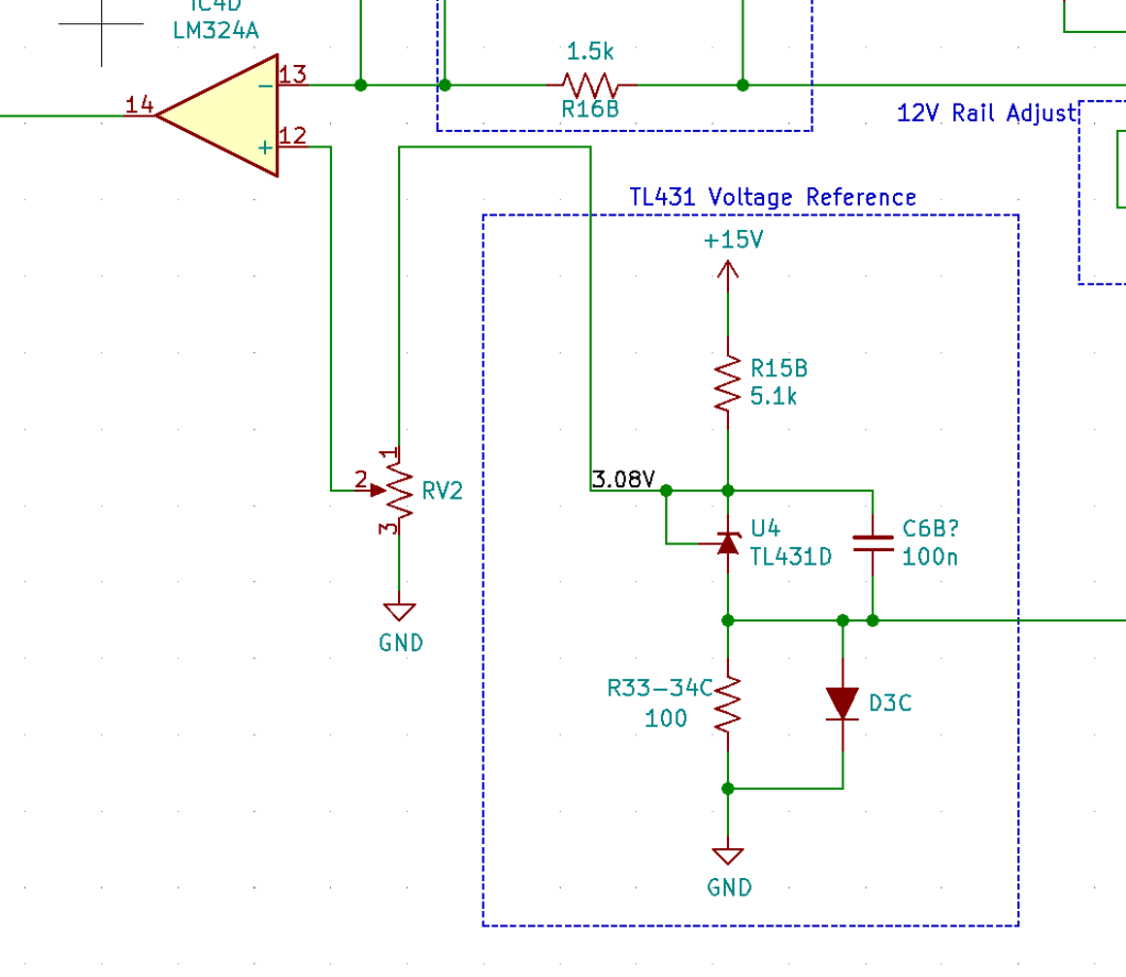
I went a bit overboard with this. One thing led to another and before after very very long I had most of the low voltage side reverse engineered in Eagle. At the time of making this project I used Eagle to do my schematic work, but have since switched to KiCAD and couldn’t be more pleased with it. I decided to take the time to recreate only the relevant circuits using KiCAD, starting with the voltage feedback path as shown below:


From right to left:
- R43B and R44B form a voltage divider which will cause a 12V input to be divided down to 11.3V and is then fed into the non-inverting input of op-amp IC2
- Op-amp IC2 drives a resistive divider formed by R37B, RV1 and R14B. This divider takes the 11.3V from op-amp IC2 and divides it down to a value between 2.38V and 3.16V (assuming VR1 is 1k)
- The above value is fed into inverting pin of op-amp IC4
- TL431 generates a precision voltage reference of 3.08V and feeds it into the non-inverting pin of op-amp IC4 to be compared to the value from #3
Op-amp IC4 compares the two voltages from #3 and #4. If the value fed into the inverting pin drops below the reference 3.08V, the output will increase in voltage and cause the opto-coupler to receive less current. This in turn causes the photo-transistor on the left to conduct less, and triggers the driving circuitry to increase the PSU’s output voltage.
Thanks to this schematic we have found the following:
- Our voltage reference for voltage feedback of the 12V rail
- A potentiometer which allows the 12V rail to be slightly adjusted
- Where pins 7 and 8 end up from the back of the PSU. Pin 7 appears to allow the 12V rail to be adjusted slightly by placing different value resistors from it to ground. Pin 8 leads to some other circuitry as well, and its function isn’t entirely clear from here.
First Modification Attempt
Earlier I mentioned that if we were able to somehow adjust the value of the voltage reference, the output will follow. We can test this theory with a potentiometer wired in at the correct place. The modification is shown below.
Op-amp IC4 is responsible for comparing the voltage reference to our 12V output, so I’ve removed R26B and replaced it with potentiometer RV2. The adjustable leg of RV2 is fed into the op-amp thereby allowing us to control how much of the reference is fed into the op-amp. This is what that looks like in practice:

I’ve flipped the riser PCB upside down so I could have easy access to both sides while it was powered. The potentiometer here is wired up in a different way than I explained because I didn’t have photos of the other configuration, but the concept is the same. Here are my findings:
- The mod works!..sort of. The voltage is adjustable with the pot.
- The power supply turns off below roughly 11.3V meaning some kind of under voltage protection is being activated
- The power supply is unstable above 13V.
- The 12V rail will go as high as 25V (oops…those 16V output capacitors don’t like that) before a secondary overvoltage protection circuit kicks in.
With that figured out, we can see that one requirement cannot be met which is having an output voltage much greater than 12V.
Another challenge now is figuring out why the supply is turning off below 11.3V. I spent some more time reverse engineering the feedback circuit board and found +12V present on pin 10 of an IC marked 1002DS. In the photo below it is labeled IC3 with pin 1 being the top right of its package:
To confirm that this pin was monitoring the output for under voltage, I first cut the trace coming from pin 10 and applied 12V from an external source to the pin itself. Cutting the trace here is important so that the applied voltage does not feedback into the existing circuitry and cause other issues (Thanks Ken!). With that complete I began reducing the PSU’s output voltage with the potentiometer. This time it went all the way down to 0V without issue confirming this was the case.

So with that the power supply’s 12V output is fully adjustable from 0 to 12V which could be quite useful on its own, but I would still like to meet the requirement of having current control.
Current Control
Right now with what we’ve figured out, the power supply is acting purely as a an adjustable voltage source. Given a change in load, the voltage remains constant while the current changes to maintain the voltage. For current sources, the opposite is true. That is, for a change in load, the current will remain constant, and the voltage across the load will change to keep the current constant.
We can approach this a few different ways. Either we can find the current sensing circuitry on the PSU itself and modify it like we did the with the voltage feedback, or we can use an external current sensing circuit and tie it into the voltage feedback somehow. When I was working on this, I took the first approach then changed to the second for a couple reasons explained later.
As usual this begins with reverse engineering more of the PCB. In this case, the starting place is obvious because we’re looking for a current sense resistor. This will be a very low value resistor, less than 1 or even 0.1 ohms and will be in the output path of the 12V rail. They are used to convert a current to a voltage, a very small voltage, which lets the feedback circuit now how much current is flowing. On the underside of the main PCB, there are actually two of them which I’ve designated R64 and R65:
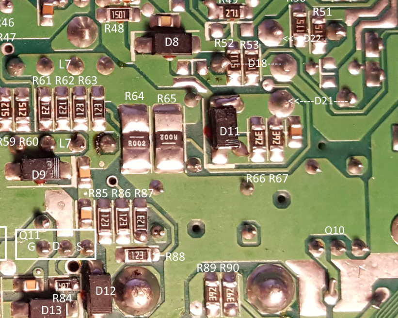
These are labeled R002 which translates to 0.002 Ω a piece. Being in parallel, they come out to 0.001 Ω. Tracing these back to the feedback PCB, I was able to come up with the following circuit:
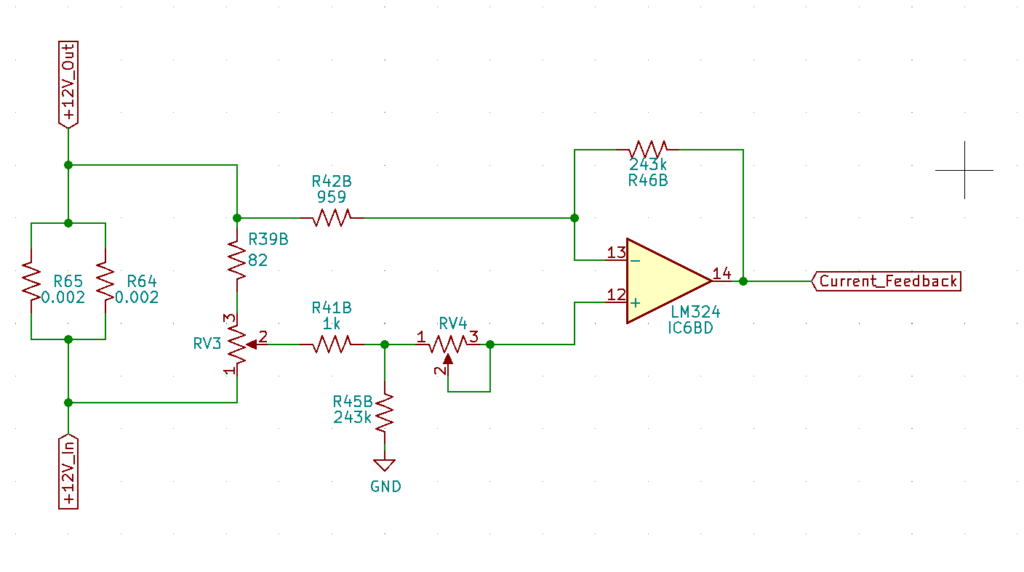
Starting on the left, current flows from +12V_In to +12V_Out, causing a voltage drop across the 0.002 Ω resistors. The specified current limit on the 12V rail is stated as 36A, therefore at full current we can expect the following voltage:
\(V = IR\)
\(V = (36A)(0.001\Omega)\)
\(V = {36mV}\)
36mV is fairly small, and to make it more useful it needs to be amplified. The above op-amp is being utilized as a differential amplifier. The generic circuit is shown below:
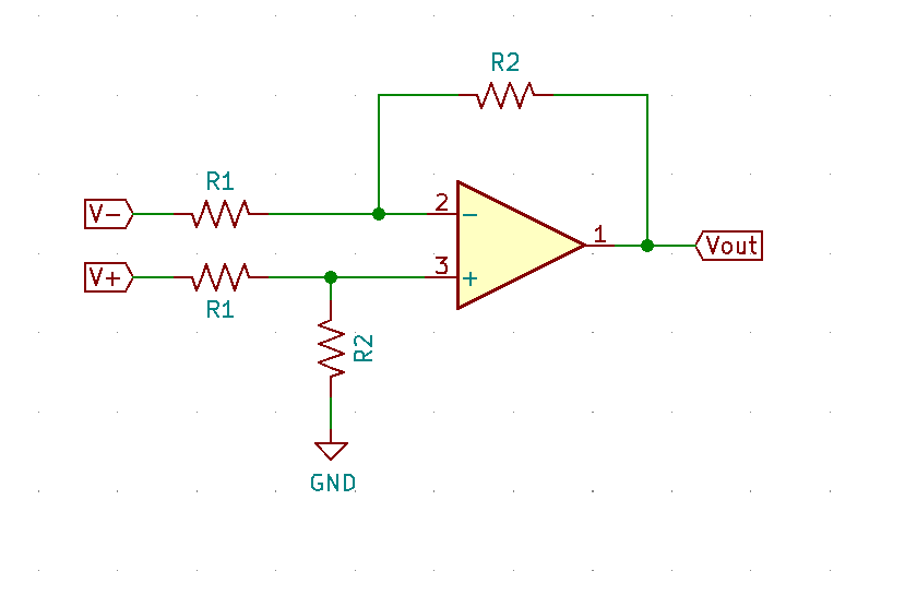
As the name states, an op-amp in this configuration only amplifies differences in V+ and V-. If a common voltage appears across both inputs, it is for the most part ignored by the op-amp and does not appear on the output. This is very useful for current sensing because in our case we have 36mV of voltage difference, but roughly 12V common to both pins. The gain, or how much the voltage difference is multiplied by is the following:
$$ \frac{V_{out}}{ V_+ – V_- } = \frac{R2}{R1} $$
R2 = 243k and R1 = 1k. Therefore the gain of the circuit is 243. So for a 36mV input, we can expect Vout=(36mV)(243), Vout = 8.75V.
This assumes both R2 resistors and both R1 resistors are extremely closely matched. Better than 0.001%. If they are not then the common voltage will start to appear on our output which is very much unwanted.
For this PSU circuit, the trimmer RV4 exists to remove unwanted DC offset from the output, while RV3 allows some adjustment of how much of the input voltage difference we want to amplify. In other words, it sets the upper current limit.
Now, just as with the voltage feedback circuitry, we can take the output of the differential op-amp and compare it to our adjustable voltage reference with another op-amp. The only problem is how do we select between voltage and current control?
thank you for this post. I bought one of these on ebay and your writing enabled me to get it to turn on. I really just wanted a 12v supply.
I do have a question about its thermal characteristics
If I just turn it on with little to no load is slowly gets warmer and eventually, the thermal protections kick in.
Is this normal and if it is, do you have a recommendation on cooling it? You allude to force airflow in your post.
Either way, thank you for the post.
Thanks for commenting and apologies for the incredibly dated reply – I was getting so many spam comments I had disabled notifications and ended up missing actual comments. What I ended up doing was mounting the PSU in an old 1U network switch chassis, and used 2x 40mm fans to pull air through the supply. They’re incredibly noisy so I had made a simple analog thermal controller using an NTC thermistor mounted inside the PSU on a heatsink. This would be covered in part 2 if I ever get around to finishing it.
Hi, This is a very nice mod for these PSUs. When you applied the 12v to IC3, pin 10 on the feedback board, would it not feed through the circuit while adjusting the pot? Also, where did you eventually take the +12v for that? I actually have one of these I may do this mod to.
Thanks, Ken
Thanks for adding about cutting the trace and where. Is there a part 2 to this? I only see part 1. Maybe I’m missing something. I’ll look again.
Thanks again, Ken
Also, Did you use a 1k pot, the same value as the resistor that you replaced for voltage control? I guess that’s only logical. I take it that the blue wire from the pot you used ,go’s to a ground point that you located. I could find any ground point, but your photo saves me some work.
Thanks again, Ken
Hi Ken, it’s only being used as a voltage divider so the exact value doesn’t really matter. 1k is a little low and might cause the potentiometer to dissipate more heat than necessary so I’d say anything from 5k to say 100k. Also for a ground point, it’s the 5th pin from the right on the “B” side of the control board. It’s labeled GND in the photo in the post.
The photo of the potentiometer I connected is misleading because that was actually an earlier attempt at a mod so it is shown connected in the wrong place. I didn’t happen to have a photo of the pot connected to the correct place, because I ended up doing this write-up over a year after I actually did this mod.
Part 2 still needs to be written up I’m afraid. I’ll try to prioritize it as it seems there is actually some interest in the project.
That small board is a real pain to remove. Using my pace desoldering machine it’s still giving me problems. Just wondering your method? I take it that the way you installed the pot is that you removed the 1k resistor that you labeled R26, and connected the wiper on the side that goes to the TL431, one end to the side that goes to pin 12 of the LM324, and the other to a ground. You had me a little confused because you labeled that pot as VR2, and there already is a VR2. Unless I am missing something.
I give you a lot of credit, you had to have spent a lot of time reverse engineering the circuit. It is very much appreciated. Still wondering if you got further on the current control and did a part 2 to this?
Thanks again!
I also struggled to remove this board myself. Some of the pins are connected to very large copper areas and really need to get a ton of heat to remove them. Sometimes it helps to put the soldering iron on the opposite side of the PCB against the pin, and the solder sucker on the bottom of the PCB so the solder melts from the rear which tends to give better results. I also recall having to use some mechanical force – wiggling the board side to side to break out any remaining pins that I just couldn’t remove all the solder out from.
I should also have labeled that pot something other than VR2 to avoid confusion. In fact, I really should have written part 1 and 2 at the same time, as this part is mostly an experimental phase of the project and was not intended to be followed. The final implementation of the voltage and current control circuits ends up being quite different than what is shown here. What is shown here works completely fine for purely voltage control, but combining it with current control forces a different approach to it.
Yes, I also had to wiggle and pull to get the board off. I also went over the pins many times and did apply heat to both sides also using some RA flux. I kept checking with a small bright LED on the back side to see which pins still had solder around them. You just have to be persistent.
I figured the current might be an issue. I might just incorporate some small dim bulbs to at least give me some current limiting if needed. A little protection.
Just a little update. Still have to remove R26 and add the pot . I have the trace cut between pin 10 and V32. I have some 28ga wire with some indestructible insulation that I soldered to pin 10. I just ran it down a out the small hole by the pins. I’m going to put the voltage divider resistors on side B after it’s soldered back in place.
I need to figure out the current control. Still wondering how it worked out. I understand what you have posted so far on the current.
I actually am going to mount just the board in a Kepco power supply cabinet. It was a 2000w @10ma that the transformer was bad. The voltage and current were not that useful anyway for what I do. I was going to try to utilize the existing circuit board with the voltage and current control, make them work with the lower voltage and higher current. It wouldn’t really work or would have been a lot of work. This will be easier. It’s in great condition. It has analog meters, but I can make them work. I’ll make the voltage 15v, and the current 40 amp. The face is really nice. Has the 2 10 turn, 5k pots. If I have to, I have a few other value 10 turn pots. I have quite a few different fans to mount in the cabinet. Hopefully will make a nice power supply. Wish the voltage would go a little higher also, but the high current will be nice to have.
That’s 2000v @ 10ma. The Kepco power supply. Not 2000w.
That Kepco sounds like a unit. Too bad it failed but as you say, 2000V is a little extreme for most hobbyist use. I’ll work on getting Part 2 up relatively soon as well since I’m getting more feedback on this. One thing for sure and I replied to another user’s comment about how these require forced air cooling – they tend to run hot just idling so some kind of active cooling is required.
Understood about the heat. I’ve been planning that out and think I’m going to put 2 fans in the unit. Like I said, I’m just going to mount the power board without the case. The top of the Kepco case has vents. I thought about putting one fan on the top blowing straight down on the power supply. Then one on the back, blowing out of the cabinet. Of course I’ll use thermistors to control them. I have a couple fairly quiet ones.
Got the pot wired in. A little hesitant on soldering that board back in yet being so hard to remove.
Do you know if I’ll need access to side A of that board if current control works out?
Hello from France
I am radioamateur, and first, my apologies for my poor English.
2 years ago, I recovered 2 P. S.’s ,exactly the same as you, and wanted to do the same job. Once the case opened … I understood my pain. So I was content to locate the rear connections (as you, même result), and I use it at 12.2 V, without current limit other than the original one, I am often afraid with that big value, and I would prefer 13.6 V ! Today, I came across your article … Extraordinary, wonderful, for me. I won’t go any further now but I also wait for part 2, and many thanks to you, I’ll re-open the beast and do the modifications. Huge congratulations on your work, everything is clearly explained, complete, precise, just what I wanted. Congratulations, and impatience for part 2.
Best regards
Bernard
Thank you for the kind words, I’m glad this work has been able to help other enthusiasts like yourself. I am also surprised how many others seems to have this model of power supply in their possession.
I soldered the small board back In and got my pot wired in. I just went ahead and connected it up to the 5k – 10 turn pot that was for the voltage on the Kepco. It’s working good. It’s going down to 67mv, and the max is 12.6v. Not bad. There are some guys doing a mod to get them up to 13.5v. Might look into that.
I bent some strips of 2mm thick copper as wide as the ground and 12v pads on the end of the board. 2- grounds and 2-12v. I had some 8ga stranded wire in black and red that I soldered each to 2 tabs. Red on top and black on the bottom. One going out each side. They’re only about 5 inches long and loop around to 35 amp banana jacks that I put in place of the original ones on the Kepco that were only required to carry 10ma. They weren’t bad jacks, but wouldn’t handle 35 amps . Maybe 10 amps.
Wish we could post photos in the comments. This could be a really nice power supply. Especially if we can get the current to work. Utilizing the 10 turn current pot. Even if we would have to make a breakout board to tie into the main board.
Hello,
Hello,
From France … A question, on these PSU (and others), just at the AC 230 V input, there are (I think) 2 + 2 varistors to limit voltage peak between line ang ground (If they are capacitors, the question is the same …) . On the PCB, line is identified “L” for line and “N” for neutral OK, but these varistors are NOT the same for line and neutral (bigger for line, it’s normal !) ).
Here, in France, in domestic normal use we do not pay attention where is neutral, and where is the line…. I never had problem, but, when such PSU are connected, is it important to always have the correct connection for line to line and neutral to neutral ? Here, In new domestic line distribution, in the wall socket, the neutral and line position are now normally fixed (?) but, in fact ?…
All my best regards and best wishes for 2021 !
Bernard
Hi Bernard,
Here in the US our N (neutral) is connected to ground in our main panel. Most of the time. Being that way we must be where of the polarity. These power supplies were designed for that circumstance.
Happy New Year,
Ken
OK, Ken, many thanks for your fast reply, and best regards !
Bernard
I to am an Amateur Radio person and I have been modding a few of the Server power supplies of different models. I stumbled across this post and found it very informative. That being said, I would really like to bump this to 13.8v and bypass the OVP circuit. I noticed the 1001DS chip and usually when you clip pin 10 on a 1002 IC chip it will disable the OVP. I have been looking at the difference between both chips, but can’t find any good information. When I clipped pin 10 on the 1001 IC, the power supply would not power up. So I am still looking for the answer. Maybe your Part 2 will cover this. Looking forward to your next post.